
As electronic devices become smaller, faster, and more powerful, manufacturers need packaging and assembly technologies that can support increasingly dense circuit designs. One technology that has become especially important for modern electronics is BGA PCB assembly.
BGA, or Ball Grid Array, is a surface-mount packaging technology that places solder balls underneath an integrated circuit rather than using traditional leads around the edges. This configuration allows manufacturers to achieve high connection density while saving valuable board space.
For electronics companies in the USA, BGA assembly can be important when developing products that require compact designs, high pin counts, reliable electrical performance, and efficient manufacturing.
However, BGA assembly also requires careful process control. Because the solder joints are located beneath the component, they cannot be fully inspected using ordinary visual methods after placement. Manufacturing processes such as controlled reflow, automated optical inspection, and X-ray inspection therefore play an important role.
What Is BGA PCB Assembly?
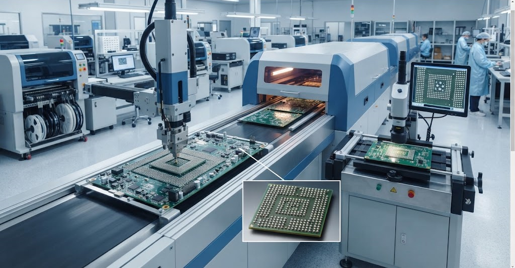
BGA PCB assembly is the process of mounting Ball Grid Array components onto a printed circuit board using surface-mount manufacturing techniques.
Unlike traditional integrated circuits with visible pins around their perimeter, a BGA package has an array of solder balls on its underside. During assembly, the component is positioned over corresponding PCB pads, and the board passes through a controlled reflow process.
Heat melts the solder, allowing the solder balls to form electrical and mechanical connections between the component and the PCB.
This design offers several advantages for high-density electronics.
According to FastTurn PCB, its BGA assembly process includes solder paste printing, automated component placement, controlled reflow soldering, and inspection using AOI and X-ray systems. The company states that its BGA capabilities support pitches down to 0.25 mm.
Why Is BGA Technology Important?
Modern electronic products continue to demand greater processing power in smaller physical packages.
Smart devices, telecommunications equipment, medical electronics, automotive systems, data-center hardware, aerospace electronics, and industrial equipment can all require highly integrated components.
BGA packages help address this challenge by providing many electrical connections in a relatively compact footprint.
High Pin Density
One of the primary benefits of BGA packaging is connection density.
Instead of placing leads around the perimeter of a package, solder balls are arranged across the underside. This allows more connections to fit into a smaller component area.
Efficient Use of PCB Space
Compact component packaging can help engineers make better use of limited board space.
This is especially useful when designing small electronic products or complex multilayer PCBs.
Improved Electrical Performance
BGA packaging can provide short electrical paths between the component and PCB compared with some traditional package configurations.
This can be useful for high-speed and high-performance electronic designs, although actual electrical performance depends on the complete PCB design and implementation.
Thermal Considerations
BGA packages can also offer thermal advantages depending on package construction and PCB design.
Thermal performance is influenced by the component, PCB stackup, copper design, solder connections, thermal vias, and the overall system.
How Does BGA PCB Assembly Work?
A reliable BGA manufacturing process requires multiple controlled steps.
1. PCB and Design Review
Before production, the PCB design and manufacturing documents should be reviewed.
Important considerations can include pad dimensions, solder-mask openings, component placement, board stackup, thermal requirements, and manufacturing tolerances.
A Design for Manufacturability, or DFM, review can identify potential issues before production begins.
FastTurn states that its DFM review examines factors such as BGA pad dimensions, solder-mask openings, and soldering-process optimization.
2. Solder Paste Printing
Solder paste is applied to the PCB pads using a stencil.
Consistent paste deposition is important because insufficient or excessive solder can affect the resulting solder joint.
Stencil design, aperture dimensions, paste characteristics, board cleanliness, and printing parameters all contribute to process quality.
3. BGA Component Placement
Automated pick-and-place equipment positions the BGA component on the PCB.
Placement accuracy is especially important for fine-pitch packages because small alignment errors can affect the relationship between the solder balls and PCB pads.
Modern SMT manufacturing equipment is designed to place components accurately and consistently.
4. Reflow Soldering
The populated PCB moves through a reflow oven with a carefully controlled temperature profile.
The solder melts and forms the connections between the BGA package and PCB.
Temperature profiling matters because the board and component need to experience the appropriate thermal conditions without creating unnecessary stress or defects.
FastTurn describes its BGA process as using controlled reflow soldering and notes that surface tension during reflow helps with component alignment.
5. Inspection
After reflow, the assembled PCB is inspected.
AOI can identify visible placement and soldering issues, while X-ray inspection can examine the hidden solder joints underneath BGA packages.
This combination is particularly useful because a significant portion of the BGA connection area cannot be directly viewed from above.
Why X-Ray Inspection Matters for BGA Assembly
Inspection is one of the most important considerations when selecting a BGA assembly provider.
With many conventional components, visual inspection can reveal problems with solder joints and component placement.
BGA packages are different.
The solder connections are underneath the package, making them inaccessible to ordinary visual inspection after assembly.
X-ray inspection provides a non-destructive way to examine the internal solder connections.
It can help identify potential issues such as:
- Voids
- Cracks
- Inadequate soldering
- Misalignment
- Bridging-related defects
- Irregular solder-ball structures
FastTurn specifically states that it uses high-resolution X-ray inspection for BGA solder joints and provides inspection reports for traceability.
Common BGA Assembly Challenges
BGA technology offers significant advantages, but it also creates manufacturing challenges.
Solder Voids
Voids are empty areas within solder joints.
The significance of a void depends on its location, size, distribution, component type, and application requirements.
X-ray inspection can help identify these internal features.
Component Misalignment
Accurate placement is essential for fine-pitch BGA packages.
Although reflow surface tension can assist with alignment, the component must initially be placed within appropriate manufacturing tolerances.
Insufficient Solder
Insufficient solder can compromise the connection between the BGA and PCB.
Solder paste printing, stencil design, pad geometry, and process control can all affect solder volume.
Excessive Thermal Stress
Improper reflow profiles can expose components and PCBs to unnecessary thermal stress.
A controlled thermal profile should be developed according to the materials and components used in the specific assembly.
Board Warpage
PCB warpage can affect how BGA packages contact their corresponding pads during assembly.
This becomes increasingly important with large boards, thin boards, multilayer constructions, and demanding thermal processes.
BGA Design Considerations
Successful BGA PCB assembly starts before the board reaches the factory.
The PCB designer should consider manufacturing requirements during layout.
Pad Design
Pad dimensions and configuration influence solder-joint formation.
FastTurn notes that it commonly recommends ENIG surface finishes with NSMD pads for BGA applications.
The appropriate design should always be confirmed against the component manufacturer’s recommendations and the PCB fabricator’s capabilities.
Via Placement
Vias near BGA pads require careful consideration.
Depending on the package and design, engineers may use different via structures or routing strategies to escape signals from the BGA area.
High-density packages can require advanced PCB technologies, particularly when routing large numbers of high-speed signals.
Trace Routing
BGA fanout and escape routing need to be planned carefully.
The available routing channels depend on BGA pitch, PCB layer count, via technology, signal requirements, and manufacturing capabilities.
Thermal Management
High-performance processors and other advanced components may generate substantial heat.
PCB designers may need to consider copper areas, thermal vias, package recommendations, heat spreaders, and system-level cooling.
Types of BGA Packages
BGA is a broad category that includes several package variations.
FastTurn lists support for several BGA-related package types, including PBGA, CBGA, µBGA, FCBGA, WLCSP, and stacked BGA packages.
PBGA
Plastic Ball Grid Array packages use a plastic package construction and are widely used across electronics applications.
CBGA
Ceramic Ball Grid Array packages use ceramic packaging and may be selected for applications requiring specific thermal or environmental characteristics.
Micro BGA
Micro BGA packages are designed for compact applications where board space is limited.
Flip-Chip BGA
FCBGA combines flip-chip technology with a BGA package structure and is used in high-performance applications.
The appropriate package depends on electrical, mechanical, thermal, reliability, and manufacturing requirements.
BGA Rework and Reballing
Even with strong manufacturing controls, BGA components may occasionally require repair or replacement.
BGA rework involves removing and replacing a component while protecting the PCB and surrounding components.
What Is BGA Reballing?
Reballing is the process of removing and replacing the solder balls on a BGA package.
It may be required when a component is being reused or when solder-ball integrity needs to be restored.
FastTurn states that its BGA rework services include solder-joint repair, component replacement, solder-ball reattachment, and PCB pad repair and cleaning.
Because BGA rework involves localized heating and precise alignment, it requires appropriate equipment and trained technicians.
BGA PCB Assembly for Prototypes
BGA assembly is not limited to high-volume manufacturing.
Prototype developers may need BGA components when validating a new product design.
For startups and engineering teams, prototype BGA assembly can provide an opportunity to test:
- Electrical performance
- Thermal behavior
- Firmware
- Mechanical integration
- Component selection
- PCB design
- Manufacturing processes
FastTurn states that it supports prototype and low-volume BGA assembly and offers rapid prototype services depending on project complexity.
Early manufacturing feedback can be valuable because design problems are generally easier to address before a product enters large-scale production.
BGA PCB Assembly for Production
Once a design has been validated, manufacturers may transition to larger production volumes.
A production BGA assembly process needs consistent material management, repeatable placement, controlled reflow, inspection, testing, and documentation.
FastTurn’s general PCB assembly capabilities include SMT, through-hole, and mixed-technology assembly, with BGA assemblies supported by X-ray inspection.
For production programs, manufacturers should also consider component availability, approved alternatives, traceability, testing requirements, and long-term supply planning.
Industries That Use BGA Assembly
BGA packages are used across many technology sectors.
Medical Electronics
Medical equipment can require compact, high-performance electronics with carefully controlled manufacturing processes.
Automotive Electronics
Automotive systems often require electronics that can operate under demanding environmental and reliability conditions.
Telecommunications
High-density processors, communication modules, and networking equipment can benefit from compact BGA packaging.
Aerospace Electronics
Aerospace applications can have demanding requirements for reliability, testing, and manufacturing control.
Data Centers
Servers, networking equipment, and other data-center hardware use advanced processors and high-density electronics.
FastTurn identifies aerospace, medical devices, telecommunications, automotive electronics, and data centers among the industries it serves for BGA assembly.
How to Choose a BGA PCB Assembly Partner
Selecting an assembly provider requires more than comparing prices.
Check BGA Capabilities
Ask about the smallest pitch, component types, board dimensions, placement accuracy, and supported PCB technologies.
Review Inspection Capabilities
X-ray inspection is particularly important for BGA solder joints.
Ask whether inspection is performed in-house and what documentation is provided.
Evaluate DFM Support
An experienced manufacturing partner can identify design issues before production.
Ask About Rework
Find out whether the provider can handle BGA rework, component replacement, and reballing if necessary.
Review Quality Standards
Ask about applicable IPC standards, quality management systems, traceability, and testing.
FastTurn states that its BGA process follows IPC-A-610 Class II and III requirements and that its quality management system is ISO 9001 certified.
What Files Are Needed for BGA Assembly?
A manufacturer generally needs complete production documentation before providing a final quote or beginning assembly.
Common files can include:
- Gerber files
- Bill of Materials (BOM)
- Pick-and-place or XY files
- Assembly drawings
- PCB design files when applicable
- Special manufacturing instructions
- Testing requirements
FastTurn’s turnkey assembly information lists Gerber files, BOM data, pick-and-place files, and assembly drawings among its production requirements.
Providing accurate and current files can reduce delays and prevent manufacturing misunderstandings.
Frequently Asked Questions About BGA PCB Assembly
What is BGA PCB assembly?
BGA PCB assembly is the process of attaching Ball Grid Array components to a printed circuit board using surface-mount assembly and controlled reflow soldering.
Why is BGA assembly different from standard SMT assembly?
BGA components have solder connections underneath the package. Because those joints are hidden after assembly, specialized inspection such as X-ray is often required.
Does BGA assembly require X-ray inspection?
X-ray inspection is widely used to examine BGA solder joints because the connections cannot be fully inspected visually. The appropriate inspection strategy depends on the product, package, quality requirements, and manufacturing process.
What is BGA reballing?
BGA reballing involves removing and replacing the solder balls on a BGA component. It can be part of a repair or rework process.
Can BGA components be used for prototypes?
Yes. BGA components can be assembled on prototype boards, although fine-pitch packages require appropriate manufacturing equipment and process control.
What is the smallest BGA pitch an assembly company can handle?
Capabilities vary by manufacturer and equipment. FastTurn states that its BGA assembly process supports pitches down to 0.25 mm.
What industries use BGA PCB assembly?
BGA technology is used across applications including telecommunications, medical electronics, automotive systems, aerospace, data centers, industrial equipment, and consumer electronics.
How can I improve BGA assembly reliability?
Start with a manufacturable PCB design, appropriate pad and solder-mask geometry, accurate component placement, controlled solder-paste printing, a validated reflow profile, and appropriate inspection and testing.
Conclusion
BGA PCB assembly is an important manufacturing technology for modern electronics that require high component density, compact designs, and advanced processing capabilities.
The technology offers significant advantages, but its hidden solder joints make manufacturing quality and inspection especially important. A reliable process should address everything from PCB design and solder-paste printing to automated placement, controlled reflow, X-ray inspection, testing, and, when necessary, professional rework.
For companies developing electronics in the USA, choosing an experienced BGA assembly partner can help reduce manufacturing risks and support a smoother path from prototype to production.
When comparing providers, look beyond turnaround time and price. Evaluate their BGA pitch capabilities, DFM support, inspection technology, quality standards, rework capabilities, documentation requirements, and experience with your type of product.
With appropriate design practices and controlled manufacturing processes, BGA technology can provide a practical foundation for compact, high-density electronic products across a wide range of industries.